Thursday, February 5, 2015

Wednesday, February 4, 2015
Difference Counter for In and Out Gates
Sometimes, we need to know whether someone is
still inside a building before it is locked. And if so, how many persons are
still inside? There can be many other similar situations for which the circuit
presented here can come handy. But it needs separate in and out gates
to work and can count up to nine persons (inside) only. Though, it
can be extended to count more.
Circuit and working
Fig. 1 shows circuit of the difference counter,
built around four ICs, for use between entrance and exit doors. Switch S1,
which is an SPDT switch, together with gates N1 and N2 of CD4011 (IC4)
generates a pulse for incrementing counter CD40192 (IC1). CD40192 is a BCD
pre-settable up/down (bidirectional) counter. The counter moves up or down with
the positive clock edges applied to its corresponding pin 5 (clock up) or pin 4
(clock down).

When you press S1, its pole comes in contact with
its terminal 3, which is connected to pin 5 of IC4. When you release S1, its
pole returns to its original position at terminal 1. Thus, for every action of
pressing and releasing switch S1, there is an increment in display DIS1 till 9.
Pressing switch S3 momentarily resets the counter to 0.
 |
Fig. 1: Circuit diagram of the difference counter
|

Fig. 2: Actual-size PCB layout for the counter
 |
Fig. 3: Component layout for the PCB
|

Switch S2 is also an SPDT switch that works
exactly like switch S1, but it is used for decrementing the count in DIS1.
Switch S2, together with gates N3 and N4 of IC4 generates a pulse for
decrementing the counter in IC1.
The outputs of IC1 are decoded by CD4511 (IC2),
which has internal 4-bit latch, decoder and output drivers. The internal latch
is always enabled because pin 5 (LE) is connected to ground permanently. The
outputs of IC2 drive common-cathode 7-segment display LTS543 (DIS1). Since pin
configurations may be different for the other displays, always check their
datasheets before use. Resistors R5 through R11 are usually in the range of 120
to 470 ohms, depending on the type of DIS1. Here, we have used 330-ohm resistors.
Power supply of the circuit is built around linear regulator 7805 (IC3). The
input voltage is applied to connector CON1 and can be AC or DC in the range
9-15V.
Construction and testing
An actual-size, single-side PCB for the
difference counter is shown in Fig. 2 and its component layout in Fig. 3.
[Mount the components on the PCB
to save time and avoid assembly errors. Carefully assemble the components and
double check for any overlooked error. Check/verify the voltages at various
points as per the table.
You may
use any type of SPDT switches (S1 and S2) to check the increment and decrement
in DIS1 display. But for practical application, S1 and S2 should be SPDT foot
switches, which could be fitted in level with the floor at the
entrance and exit doors, respectively]
NEWS : Step out of Google Search, Try PW Beacon
One fine day, you are in a cab and you see a big banner of
your favorite singer coming in town for a concert. You pull out your phone and
start searching on the web to purchase the concert ticket. In ninety percent
of these cases, you have to take help from Google. But it has gotten old school
now, with a new IoT product called as Blesh.
Blesh, a physical web search beacon (PW
Beacon), works as a communication medium for those things that users see along
a path or a street – it just broadcasts information onto a device.. Let us say
you are at a bus station and this beacon is present there. Whenever you are
nearer to the beacon, it will flash a notification on your smartphone. You just
have to click the notification and all the
information regarding the calendar, timing schedule of the buses going to and
from that particular bus station will be displayed on your smartphone.
You can also book your bus at the same instance as that of purchasing a ticket
for a concert.

Blesh can be used near subway posters, large
banners along the street, airports and railway stations, ATMs, etc. In homes it
can be used with a secure password unlike the open version used in
public.
They work utilizing one-way communication – they transmit
signals, but don’t receive it, thus protecting the user’s information and privacy by not collecting any information
unlike what Google does. The most advantageous feature of this product is that
it boasts a two year battery life, which is enough for one to not worry about
the working of the beacon.
Speed Controller for Small Cooling Fans
Small cooling fans are used in some equipment for cooling semiconductor devices. The circuit given here is of a simple automatic speed controller for a 12V, 0.6W (or 1.2W) cooling fan that increases the fan’s speed when temperature rises, and vice versa.
Circuit and working
Fig. 1 shows circuit diagram of the speed controller for a small cooling fan. Resistor R1 limits the initialcurrent for the motor and lowers the speed of rotation, if needed . The temperature control is done with one or more NTC (negative temperature coefficient) thermistors connected in series with the electrical motor. The number of thermistors depends on their power dissipation.
Usually you cannot find low-cost NTCs with enough power dissipation. Therefore four of them in parallel are used here. This way power dissipation and self-heating of the NTCs are reduced. It is better to use NTCs with tolerance of ±2%. The NTCLE100E3 are available with nominal values of 3.3-ohm to 470-kilo-ohm and have maximum power dissipation of 0.5W at +55°C.Table I shows easily-available NTC thermistors that can be used in the circuit. The resistors R2 through R5 are equalisation and limiting resistors. These resistors are usually between 3% and 15% of the resistance of the thermistors at +25°C.
LED1 is used as power on/off indicator for the circuit. LED2 indicates the speed of rotation of the fan. If speed of the motor is high, LED2 glows brightly, and vice versa. Diode D1 is used to prevent back EMF when power supply is removed.
Connector CON1 is used for the power supply. It is better to have power supply 10 to 25% higher than the nominal working voltage of the fan to compensate for the voltage drop across the resistors and the thermistors.
Voltage drop across resistor R8 is proportional to the current in the motor. Connector CON2 is used to connect a digital voltmeter to measure the voltage drop.
Construction and testing
An actual-size, single-side PCB for the circuit is shown in Fig. 2 and its component layout in Fig. 3. After assembling the circuit on a PCB, enclose it in a suitable plastic box.
Circuit and working
Fig. 1 shows circuit diagram of the speed controller for a small cooling fan. Resistor R1 limits the initial
 |
 |
Connector CON1 is used for the power supply. It is better to have power supply 10 to 25% higher than the nominal working voltage of the fan to compensate for the voltage drop across the resistors and the thermistors.
Voltage drop across resistor R8 is proportional to the current in the motor. Connector CON2 is used to connect a digital voltmeter to measure the voltage drop.
Construction and testing
An actual-size, single-side PCB for the circuit is shown in Fig. 2 and its component layout in Fig. 3. After assembling the circuit on a PCB, enclose it in a suitable plastic box.
 Fig. 1: Circuit diagram of the speed controller |
 Fig. 2: An actual-size PCB for the speed controller |
 Fig. 3: Component layout for the PCB |
Fix all the four NTC thermistors (NTC1 through NTC4) at appropriate locations, within the equipment whose heat is to be dissipated, for temperature sensing. On front panel of the speed controller fix switch S1 for power on/off, LED1 for power on/off indication and LED2 for fan-speed indication. Before using the circuit, verify that voltages at various points in the circuit are as per Table II.
Tuesday, February 3, 2015
Make Your Own Function Generator
We’re back to discuss another circuit. This week we will see an interesting circuit which most design engineers, test engineers, hobbyists, lab technicians and students can relate to. Yes, let’s build a simple function generator. It won’t be a very high-end design but easy enough to be constructed by you in the lab – real or virtual!

Function Generator Block Diagram
So what is the principle behind this function generator ? It is made up of various parts which are all op-amp circuits. The first part of the circuit is an astable multivibrator. This will generate a square wave which will oscillate between positive and negative saturation. This square wave is passed on to an integrator. The integral of a constant say ‘c’ will be c*t where ‘t’ is time across which the integration is taken place. This means that a positive constant will give a positive ramp and a negative constant will integrate to a negative ramp. Adding them together we get a triangular wave. We got our square wave and triangular wave – if only there were a way to obtain a sine wave too from this setup. Well there is. What will happen if you integrate the above triangular wave? A triangle wave consists of positive and negative going ramps. A ramp is a function that increases linearly with time. If you integrate a ramp, you get a function that increases as the square of time which has the shape of a parabola. So the integral of a triangle wave is a series of positive and negative going parabolic shapes. In other words, yes you guessed it right you will get a pretty accurate sine wave. Alternatively I can approach this mathematically. We have to integrate the ramp c*t – which would result in c*t2/2. As you can see integration reduces the amplitude of the result. This can be adjusted by inserting an amplifier at the end.
Let’s take a look at the circuit:

Function Generator Circuit
Starting from the left hand side, the first portion is an astable multivibrator, the output of which is a square wave. R0 is the feedback resistor and C0 is the timing capacitor. The frequency of this square wave can be varied by varying the RC values namely the R0 and C0 values. Note the initial value of capacitor C0. It is set to 1 V. In real life the oscillations will be started by the offset voltage inherent to op-amps which would charge the capacitor and in turn push the output to positive and negative saturation. But since we are using an ideal opamp this ‘irregularity’ is introduced by giving an initial voltage to the capacitor.
This square wave is applied to an integrator as shown which in turn converts the square wave to a triangle wave.
Further the triangular wave is integrated again through another integrator resulting in a sine wave. The output of this integrator is connected to an inverting amplifier with gain given by -R10/R9. Varying this gain you can control the amplitude of the sine wave.
Let’s see the output when you simulate the given circuit:

Function Generator Output
So without the help of any external input source using only the op-amp and the supply provided to it we have generated three standard waveforms. This is the principle of working of the basic function generator you find in your lab.
How stuff works : Your cell phone charger
In today’s mobile age , our cell phones keep us connected to everyone 24×7. Without mobiles, we’ll all be back to the Stone Age. But irrespective of their class, they all run on a battery which goes down at the end of the day. The smarter your phone, the sooner it runs out of charge.

Have you ever wondered about the one thing that keeps your phones going? Yes, we are talking about your cell phone chargers here. Cellphone chargers are nothing by simple AC to DC converters, i.e. they take the regular AC supply of 220/120 volts coming to our homes, and give a constant DC output voltage of around 5 V (approx). In this article, we are going to talk about the internals of a cellphone charger and even create a working circuit.
The cellphone charger extracts the power from the home supply (AC 220V) and converts it to a DC level of required voltage. The voltage output is fairly constant which means it is regulated. The output voltage remains constant whether the load current changes or there are fluctuations in the input AC voltage. This is achieved in a series of steps:
Step 1: Step down the high input of 220V to a working output voltage. This is achieved with the help of a transformer
Step 2: Convert AC signal into a DC signal using rectification
Step 3: Smoothen the output of the rectifier by filtering the ripples from DC rectification
Step 4: Generate a steady output signal with the help of a regulator
The circuit below gives a high level view of the working of a “regulated power supply”.
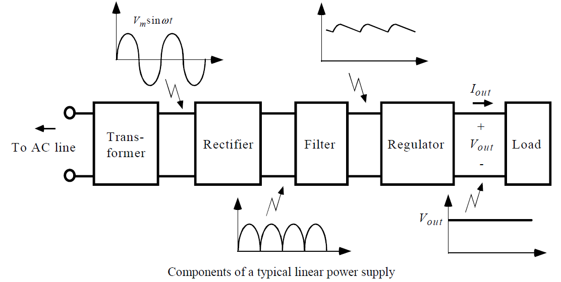
The components used are very common and simple. Most of you know what goes on inside of them.
Transformer:
The transformer contains two huge copper coils, one between the two terminals of the input power supply and other between the two terminals of the output. Here we use a step-down transformer which means it will convert high voltage to low voltage. The number of turns of the coil inside will determine the voltage supported at input and output both.
i.e. Vin/Vout=Nin/Nout
Vin = Input AC voltage
Vout = Output AC voltage
Nin = Number of turns at the input terminal of transformer
Nout = Number of turns at the output terminal of transformer
Rectifier:
Now comes the rectifier part. This converts the AC voltage output of the transformer to a DC voltage. It just reverses the polarity of one half of the period of the AC signal. This will make both parts have the same polarity. Here we use a full wave bridge rectifier to convert the AC signal to DC.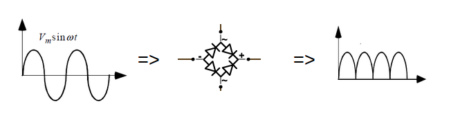
Filter:
The output from the rectification stage is DC, but hardly constant. So, we use capacitive filtering to smoothen the output. In this example, using a simple low pass filter at the output of the rectifier, however in real life, higher order filters may be used, which would give a much more smoother output.
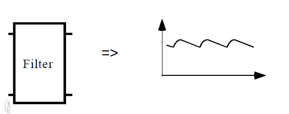
Regulator:
The filtering significantly smoothens the output, but even after that small ripples remain. If we use this directly to charge our phones, the constant fluctuation in the voltage may damage the device. It is very important to have a steady output voltage with minimal fluctuations. This is where the regulator stage kicks in.
Here we have used a simple zener diode based regulator. The tendency of a zener diode is to have a fixed voltage between its two terminals when reversed biased. So when input voltage changes, the current through the zener diode also changes inversely so that the output is constant. This regulator is quite simple to create, but its is that it wastes a lot of power. So, the cell phone chargers typically use IC voltage regulators, such as IC 7805, IC 7806, IC 7812 etc.
Combining all the steps explained below, here’s a working circuit for “regulated power supply”. You can even go ahead and run it with DoCircuits and see it working for yourself !!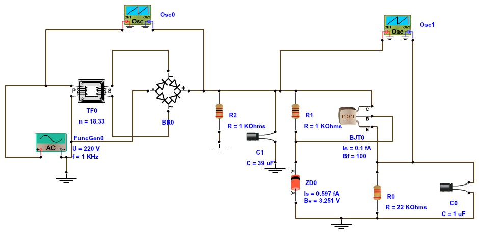
All the symbols have their usual meanings. Function generator is used as a power input source to the system. OSC1 and OSC2 are the CRO’s placed at the input and at the output terminals and can be used to study the changes between them.
So, hope you will now appreciate the small charging device at your home a little better, and if it breaks down, don’t hesitate to open it up and pry upon the internals. Even if you want some unique voltage supply, you can custom build it so easily now. But like any other technology, people are revolutionizing this as well. We’ll leave you with a glimpse of the same:
Please do share your comments and feedback
Subscribe to:
Posts (Atom)